STM32 Smart Watch
High-Speed Memory, Power Integrity & Embedded Hardware Design
Description
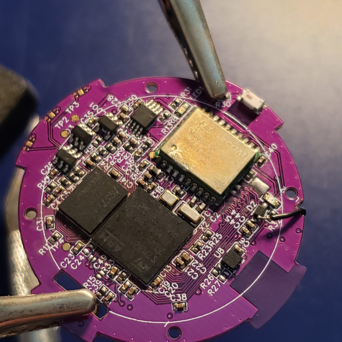
A custom smart watch built around the STM32L4R9 microcontroller, designed as a deep exploration into high-speed memory interfaces, mixed-signal PCB design, power integrity, and dense embedded system integration.
This project targeted features useful for running and physical activity while pushing the limits of a four-layer PCB with high-speed peripherals such as PSRAM, MIPI display interfaces, Bluetooth audio, GPS, and removable storage.
Project Overview
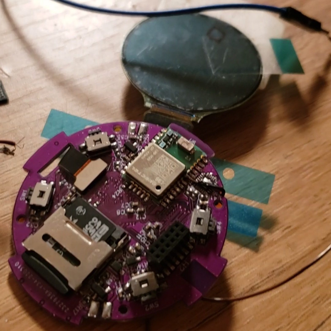
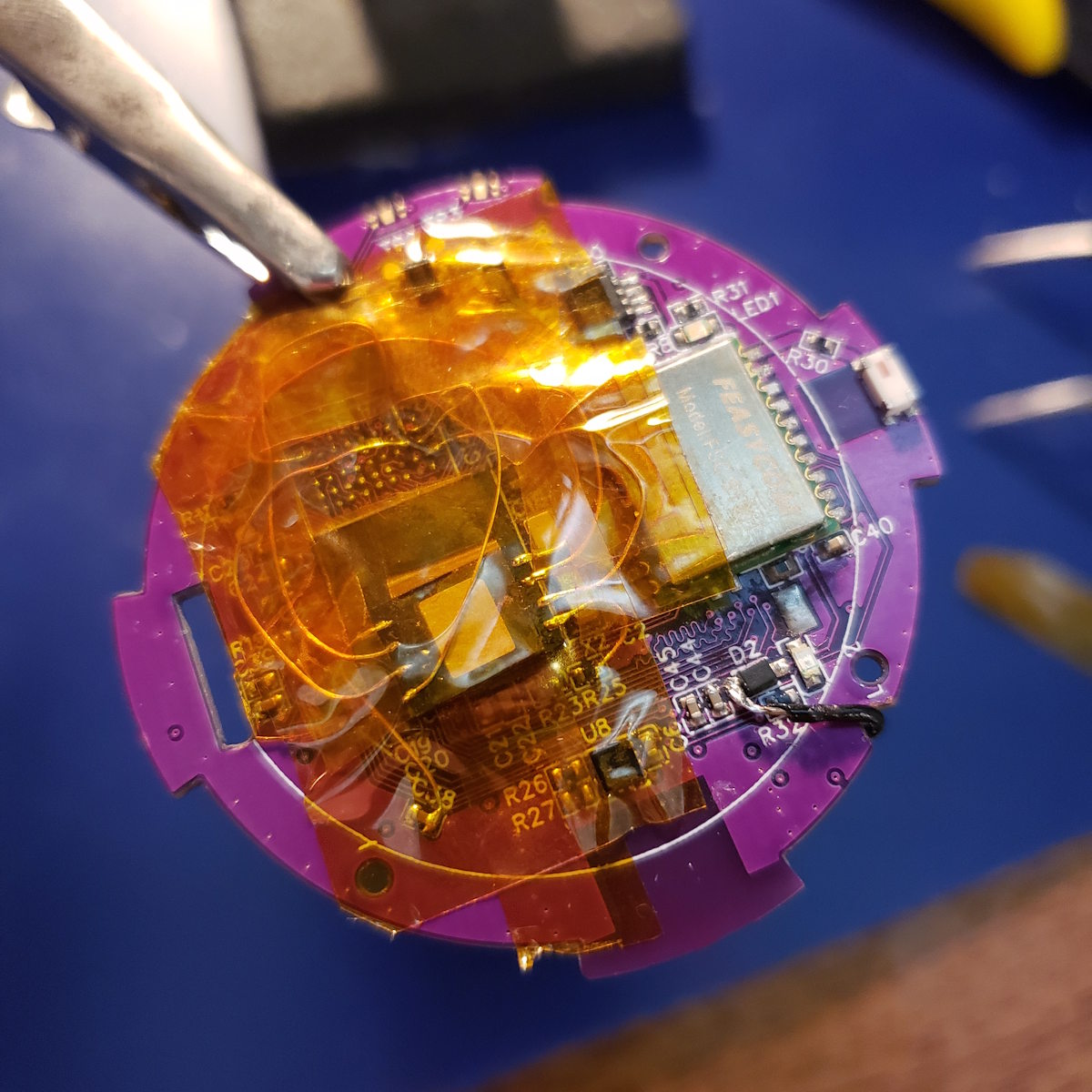
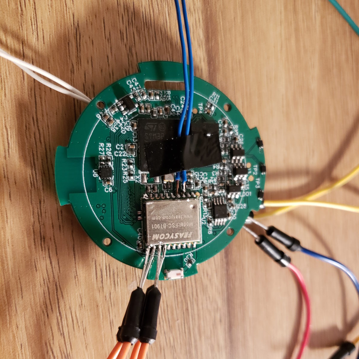
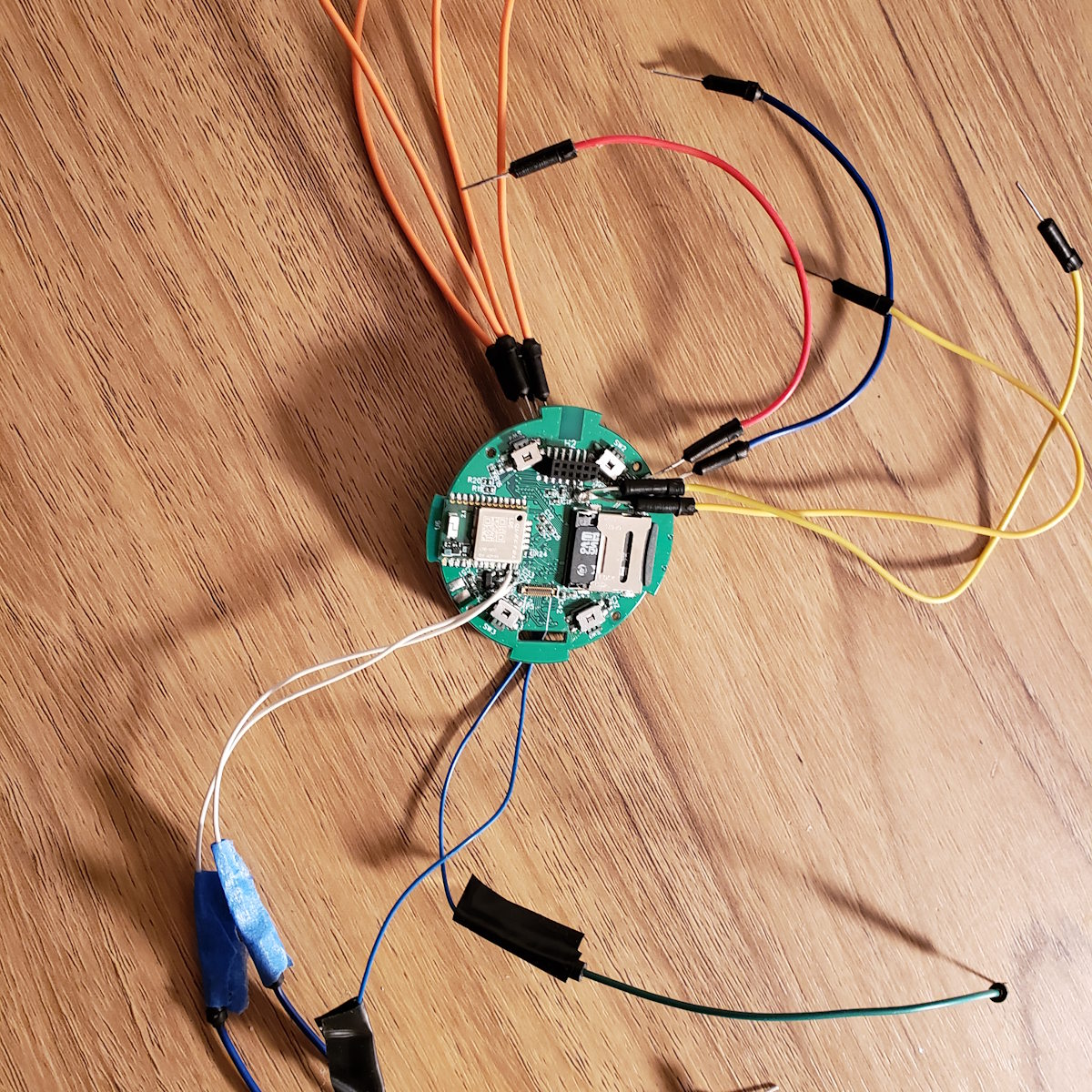
The smart watch integrates a wide range of subsystems into a compact wearable platform: external PSRAM for framebuffer storage, a high-resolution display, Bluetooth audio streaming, GPS positioning, SD card storage, sensors, and battery charging circuitry.
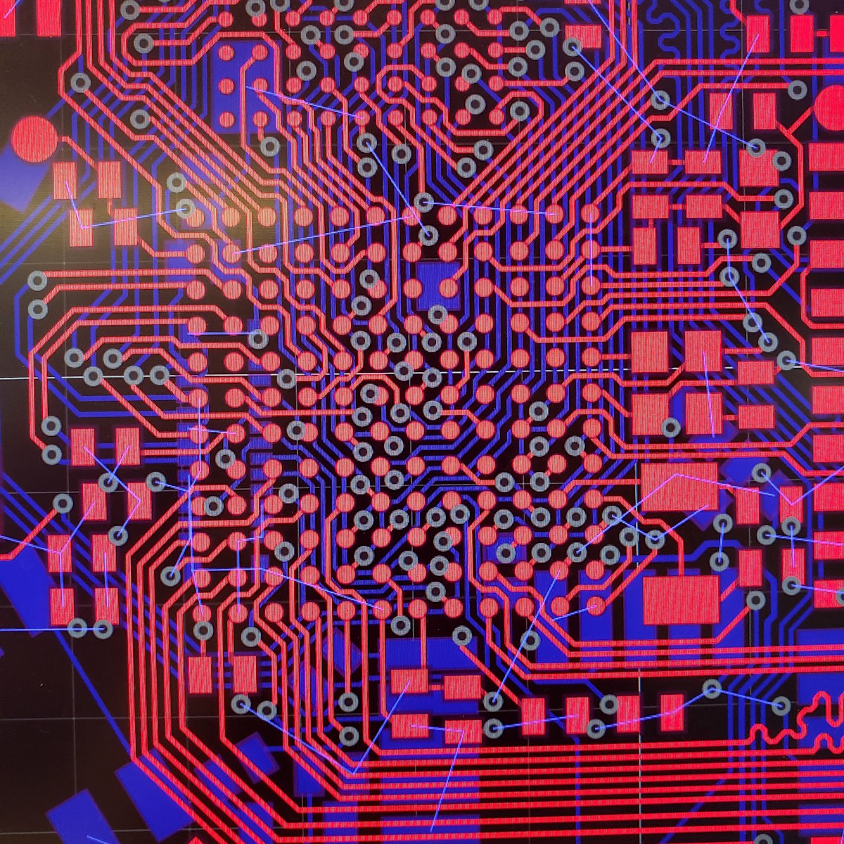
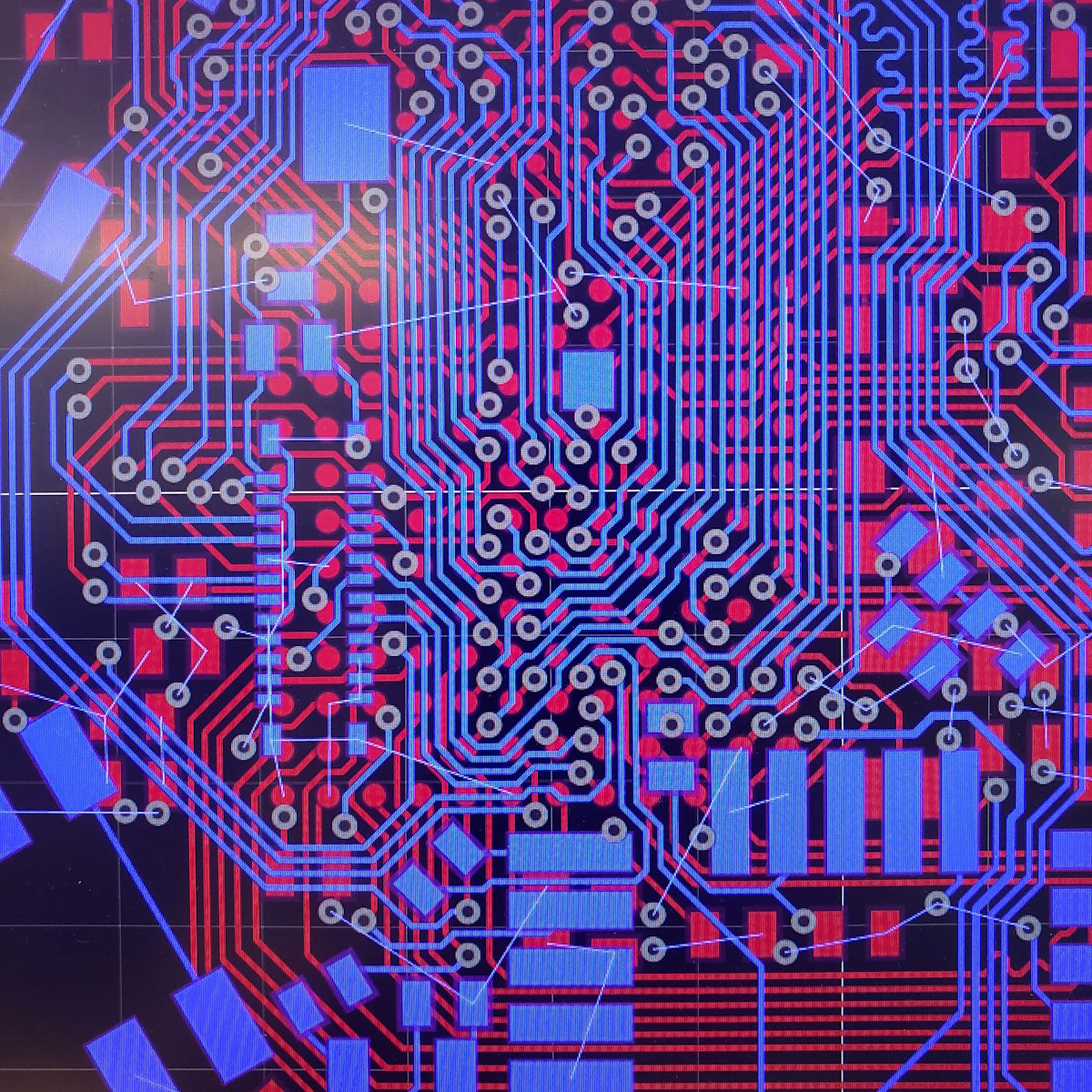
A major focus of the project became diagnosing and solving hardware-level failures — including power rail collapse, memory timing constraints, FMC interface conflicts, and connector pinout mismatches — all of which required board rework, redesigns, and careful signal analysis.
Features
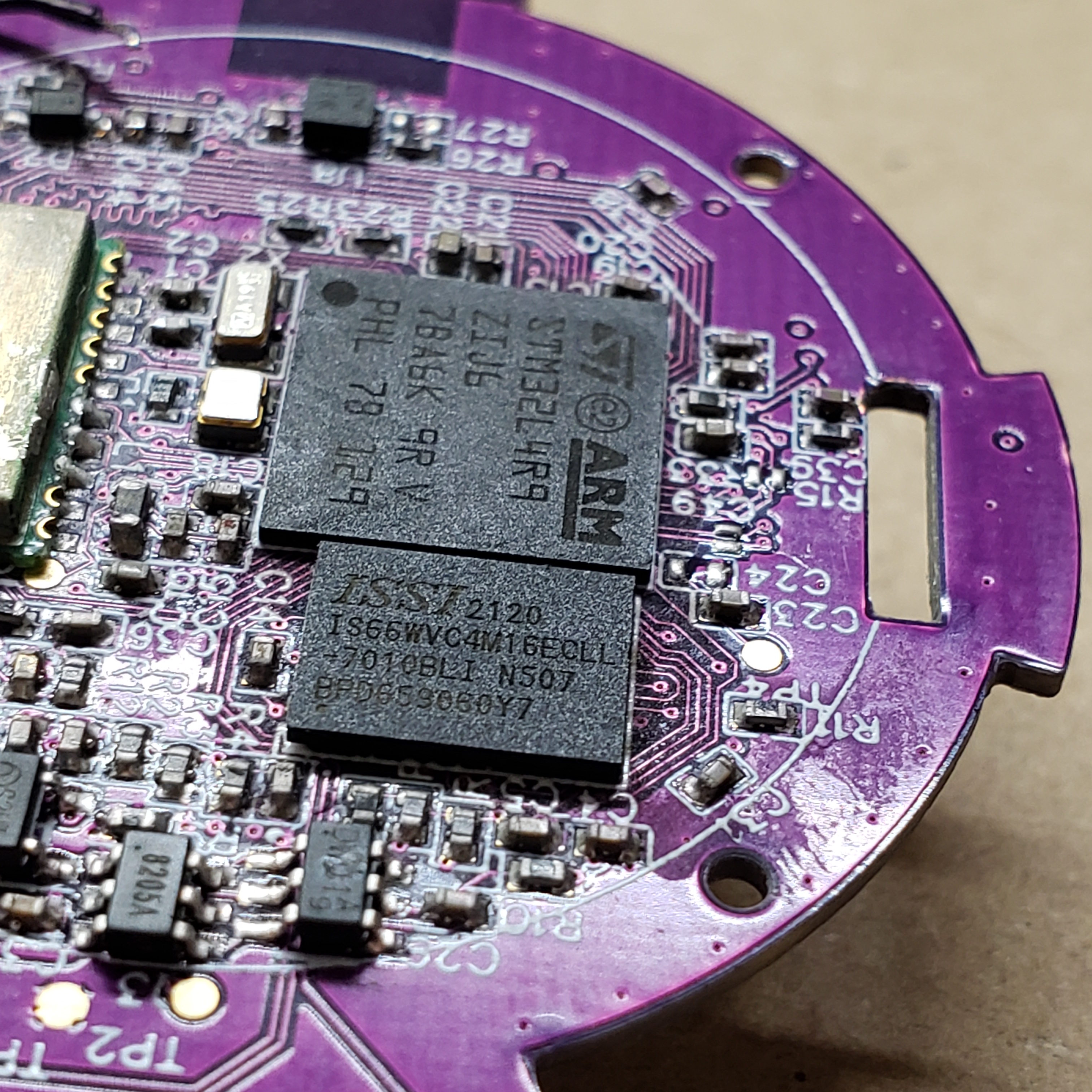
- STM32L4R9 microcontroller
- MIPI display interface
- 64Mbit external PSRAM
- Micro SD card storage
- Bluetooth A2DP audio transmit & receive
- GPS module for positioning
- Rotating bezel using hall effect sensors and magnets
- 4 physical buttons
- Accelerometer
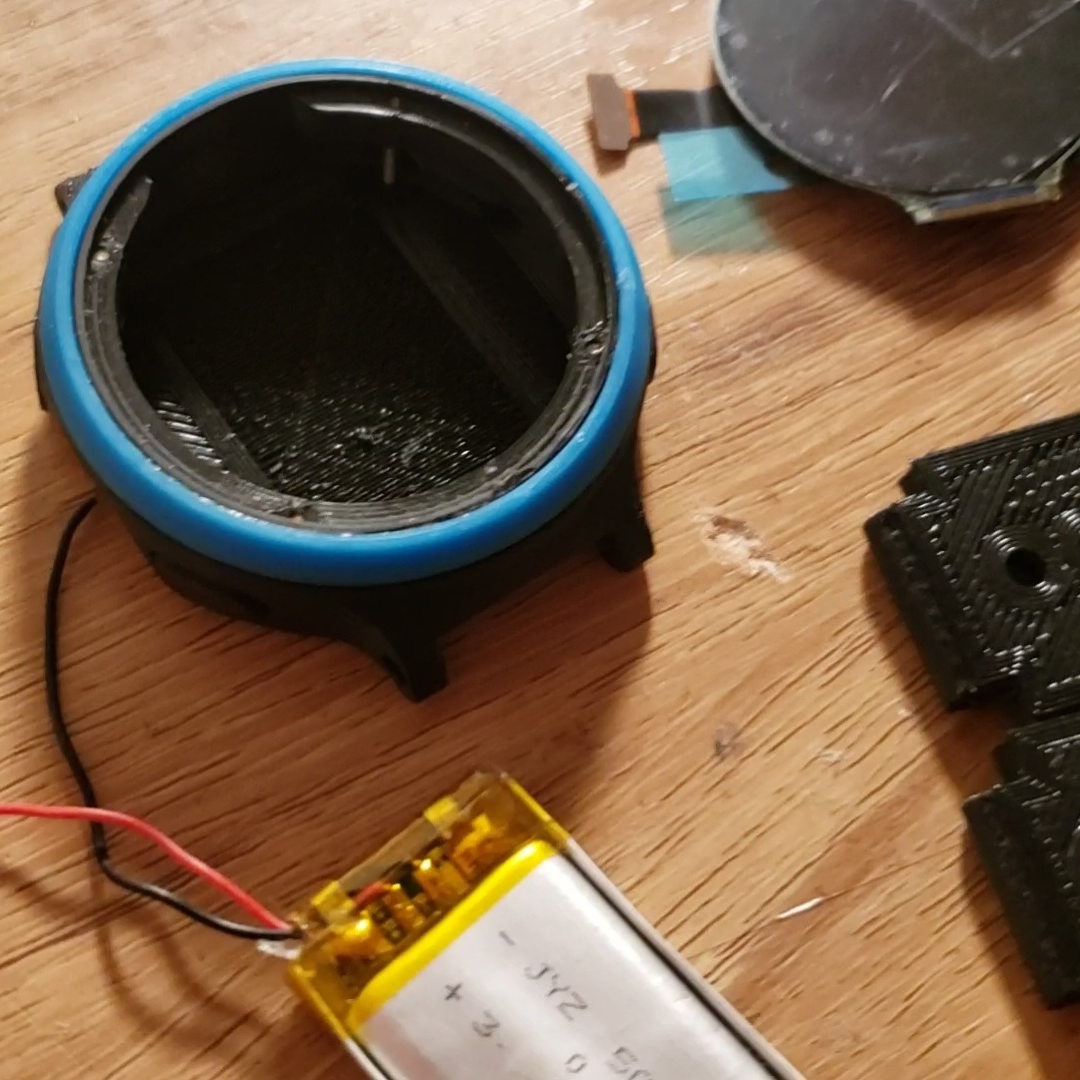
- Battery charging and power management
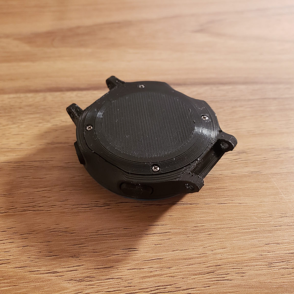
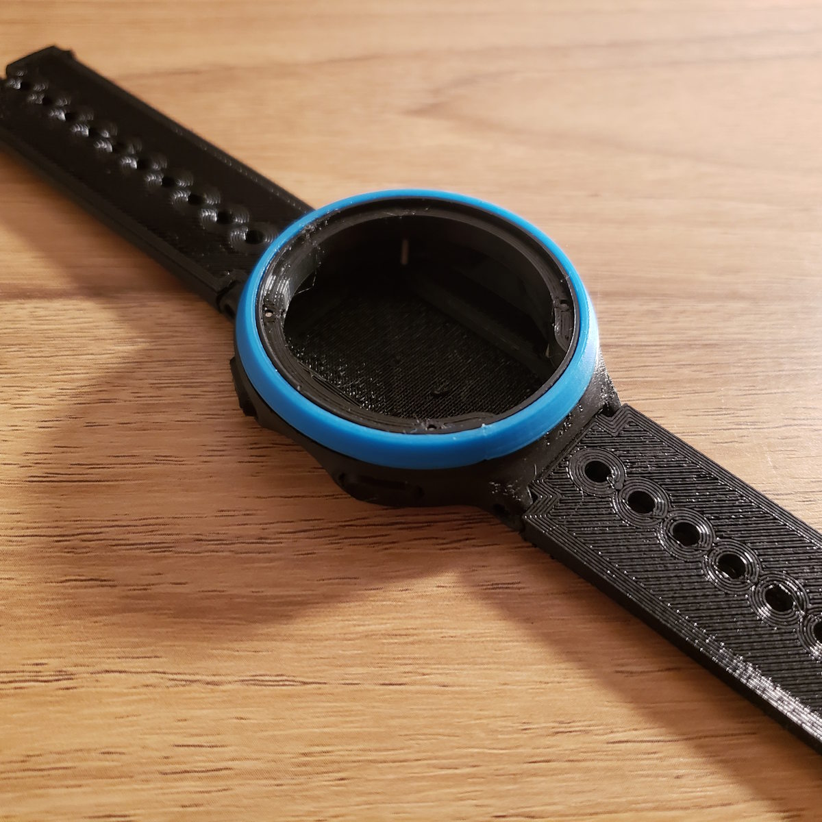
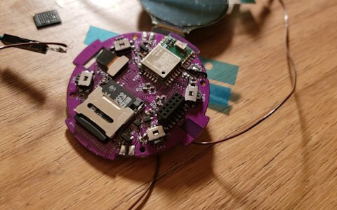
- Custom mechanical case design
Challenges & Hardware Debugging
- External PSRAM Timing: Discovered incompatibilities between STM32 FMC minimum page size and PSRAM page boundaries, preventing intrapage reads and limiting achievable performance.
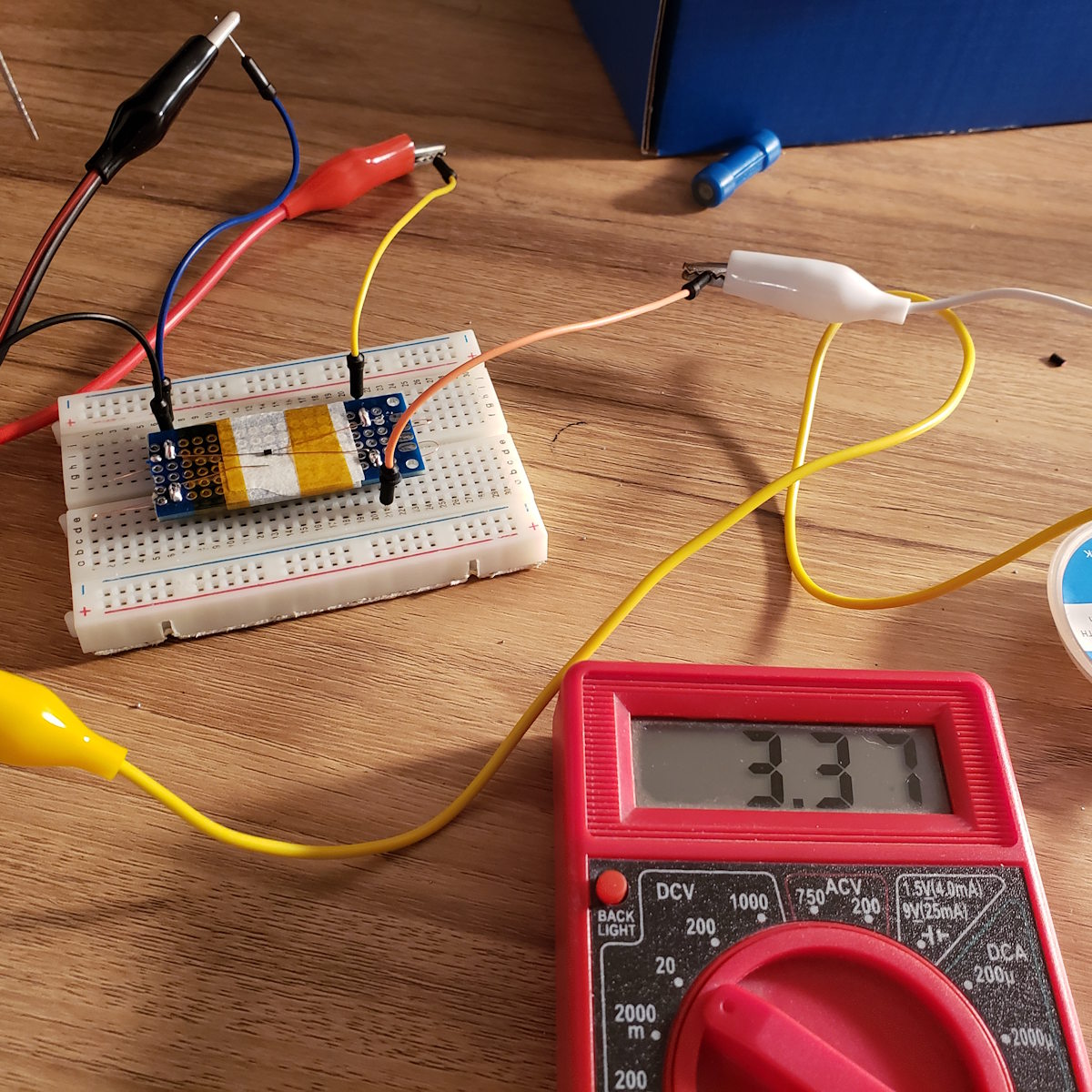
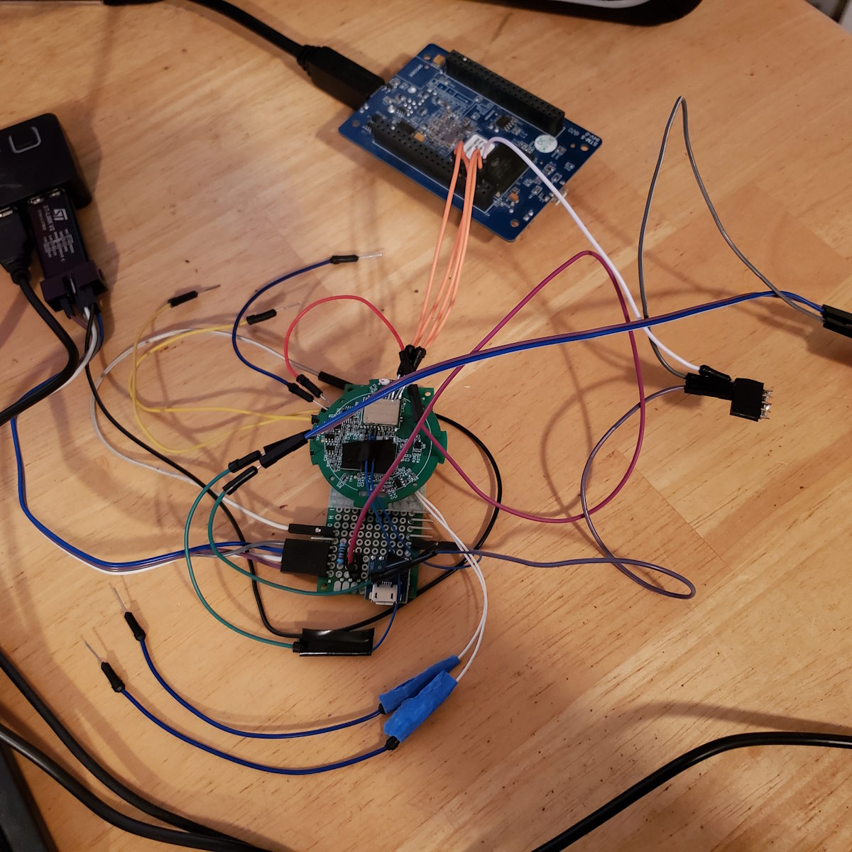
- Power Rail Instability: Severe 3.3V noise and voltage collapse observed when connecting the display. Diagnosed using an Arduino as a live voltage monitor and traced back to misuse of the battery charging IC.
- Display Short Circuit: Screen caused a direct short to ground. Root cause identified as an incorrect connector pinout due to visually identical displays with incompatible pin mappings.
- Board Redesign: Required a second PCB revision to support the correct display connector and a new PSRAM chip with different interface requirements.
- FMC Signal Conflicts: SPI and FMC pin multiplexing conflicts, including NWAIT and hardware TE signals, required reassignment and rerouting.
- High-Speed Signal Integrity: Four-layer PCB design required careful attention to signal integrity and layout practices.
Design & Diagnostic Process
Debugging focused heavily on power integrity and signal behavior. Voltage rails were monitored under load, revealing that the charging IC was never intended to power the full system directly. A diode-OR solution was proposed to allow the LDO to pull from the highest available source.
Memory performance limitations led to extensive research into PSRAM access modes, page boundaries, and FMC timing. Later revisions explored higher performance burst-mode PSRAM options at the cost of increased complexity.
The display failure required manual continuity testing of the FPC connector, reverse-engineering the pinout, and identifying the exact panel variant before proceeding with a compatible redesign.
Project Video
Demonstration of SD Card DMA BT music playback.
Archived
I archived this project in May 2022 as I had worked on it for several years and had plans to serve a mission for the church of Jesus Christ of Latter-day Saints.
After I returned from a mission, I picked up other projects instead. I hope to pick up this project again in the future.
Project Links
Project Files (Google Drive) →Hardware & PCB Gallery