STM32-Based Digital Oscilloscope
PCB, Firmware and Case Design
Status:Completed

Description
This project includes hardware, documentation, and other components needed for an oscilloscope build around an STM32F303RE microcontroller. It is build upon, and inspired by, the EMBO (EMBedded Oscilloscope) project by Jakub Pařez.
Project Overview
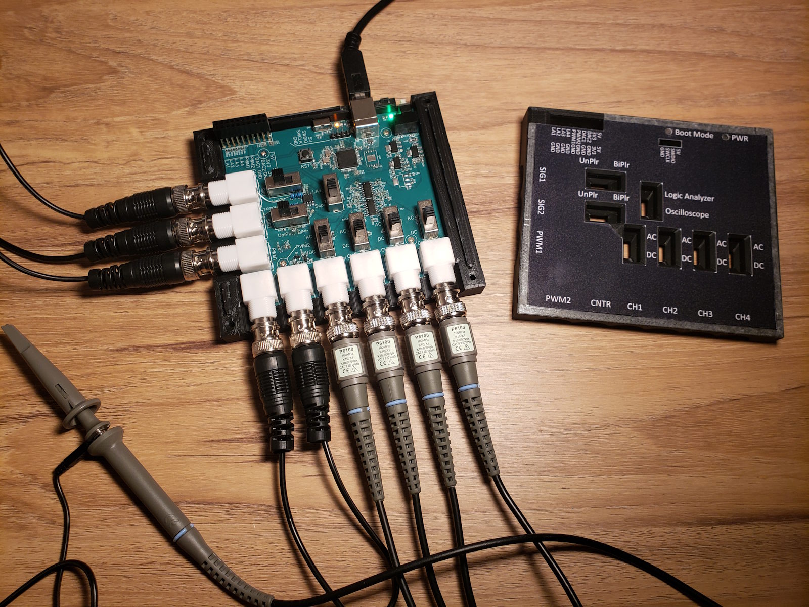
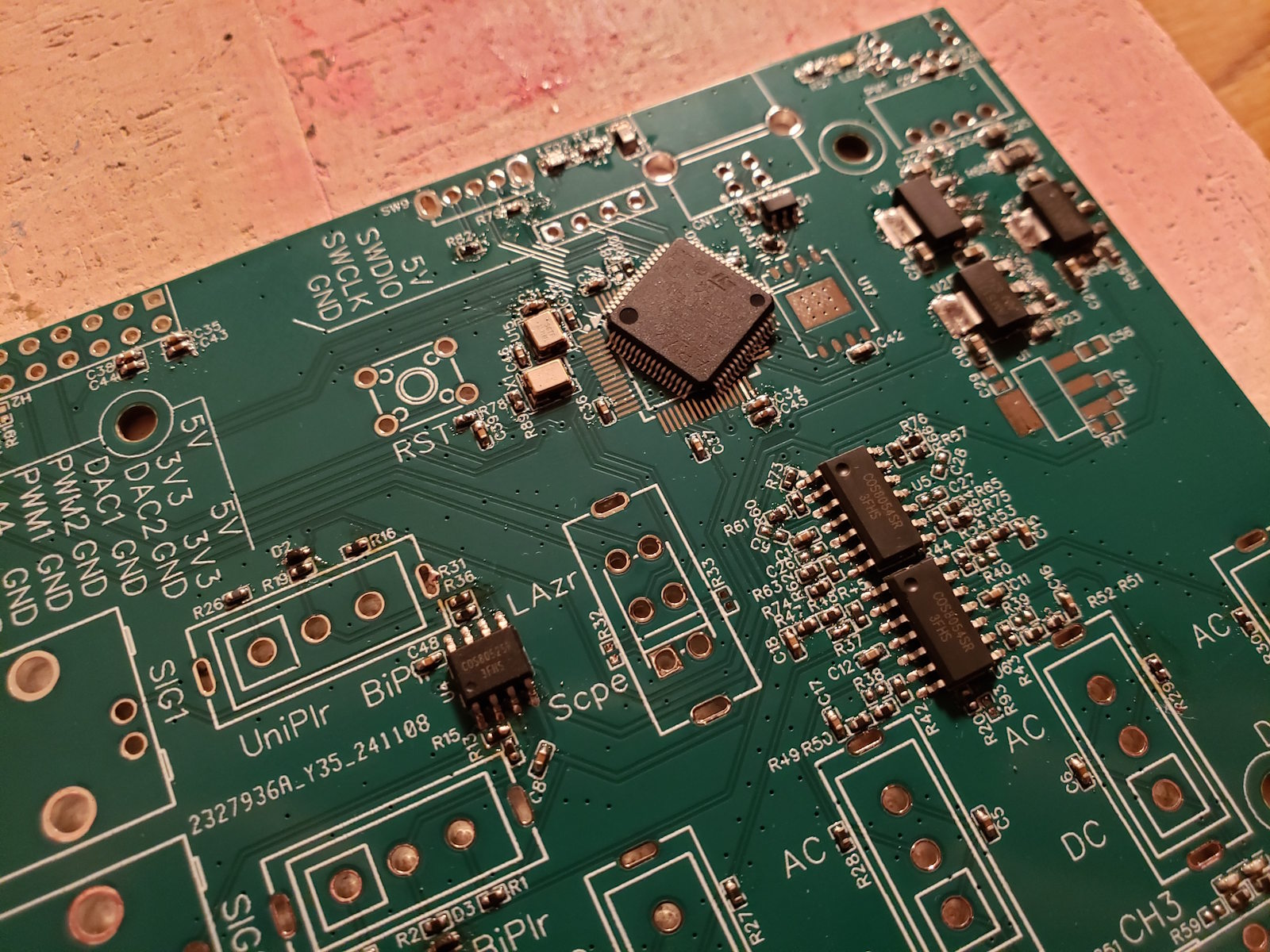
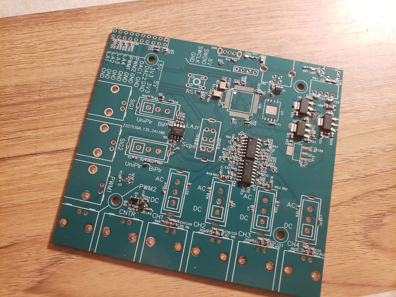
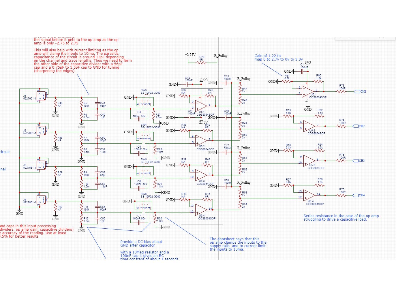
The oscilloscope is built around an STM32F303RE and provides multiple measurement instruments including a multi-channel oscilloscope, logic analyzer, signal generator, voltmeter, counter, and PWM generator. A major design focus was creating robust analog front-end circuitry capable of handling wide voltage ranges while maintaining signal integrity.
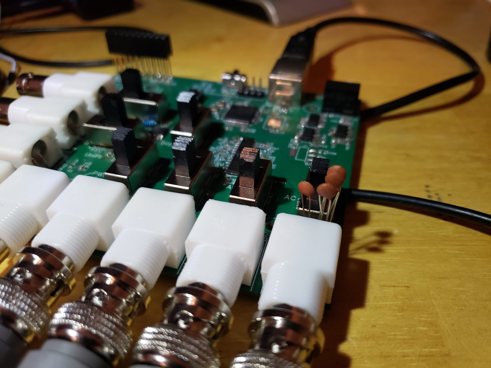
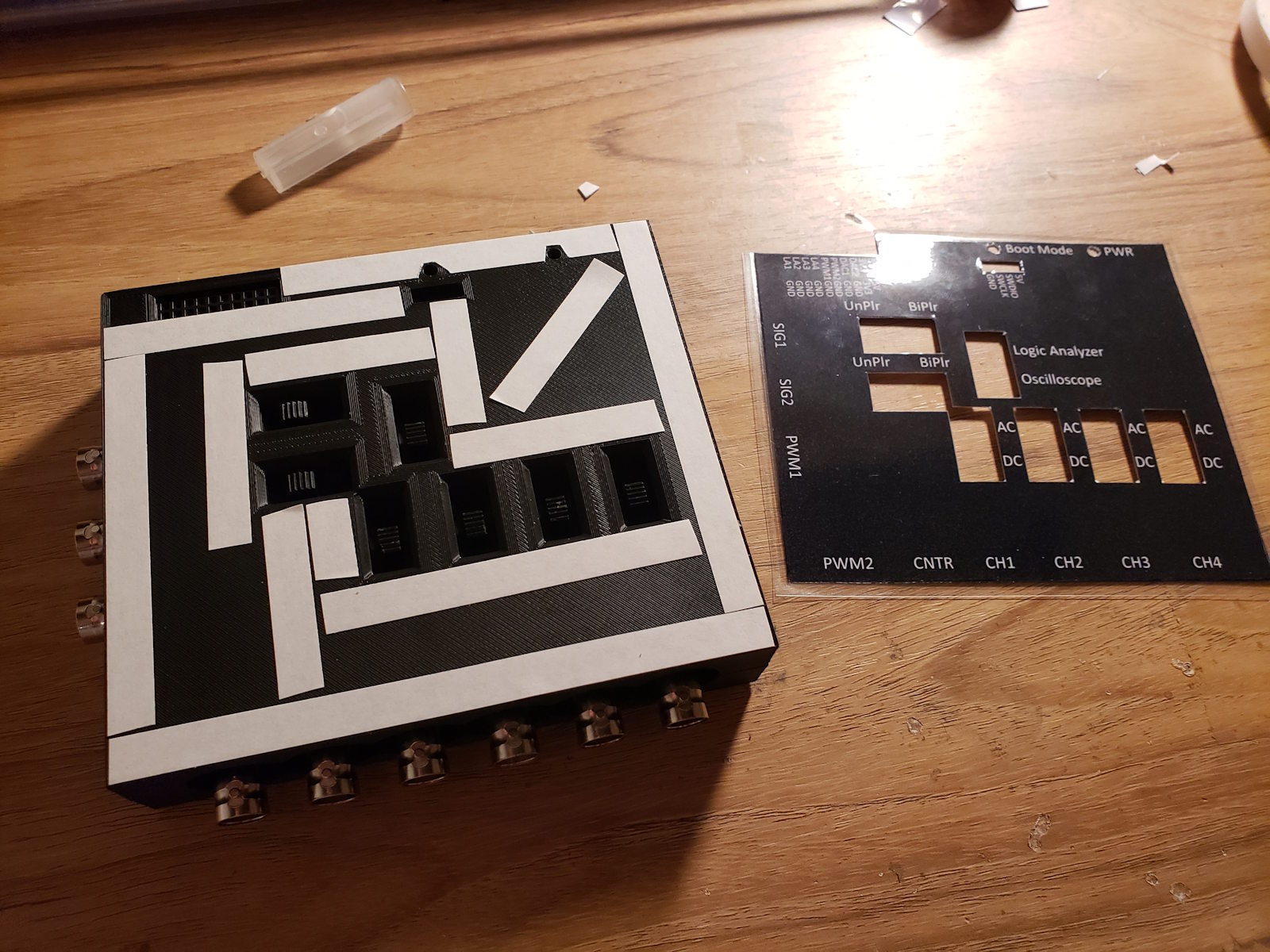
The hardware was designed as a custom PCB with BNC inputs, AC/DC coupling, configurable voltage ranges, overvoltage protection, and careful attention to PCB layout practices for mixed-signal performance. In addition to the hardware, the project includes firmware modifications and a custom USB-based workflow that simplifies software installation for the end user.
Hardware Features & Capabilities
- 4-channel oscilloscope up to 3.2 MSps (5 MSps max, limited by stability)
- 44k samples (8-bit) or 22k samples (12-bit)
- 1 MΩ input impedance with ~12 pF input capacitance
- BNC inputs compatible with standard oscilloscope probes
- AC or DC coupling selectable via hardware switch
- Configurable input voltage range (default ±3.3 V)
- Overvoltage and undervoltage protection on inputs
- Dual-channel signal generator up to 4.5 MHz
- Logic analyzer (14.4 MSps), voltmeter, counter, and PWM generator
Design Challenges & Debugging
- Implementing a resistor-capacitive divider to compensate for parasitic capacitance
- Managing op-amp stability when driving capacitive STM32 ADC inputs
- Dual power rail for bipolar voltage sensing about GND
- Reverse Engineering original Firmware and adding a secondary firmware
Design Walkthrough & Engineering Decisions
In this video, I walk through the hardware design, schematic decisions, PCB layout considerations, debugging process, and firmware architecture. The discussion focuses on real-world challenges such as parasitic effects, signal integrity, and firmware patching techniques.
Project Resources
GitHub Repository →Hardware Design & Assembly Gallery